SiGe vs. Si Selective Wet Etching for Si Gate-all-Around
p.107
p.107
A New Method to Fabricate Ge Nanowires: Selective Lateral Etching of Gesn:P/Ge Multi-Stacks
p.113
p.113
Customized Chemical Compositions Adaptable for Cleaning Virtually all Post-Etch Residues
p.121
p.121
Low Temperature SiGe Steam Oxide - Aqueous Hf and NH3/NF3 Remote Plasma Etching and its Implementation as Si GAA Inner Spacer
p.126
p.126
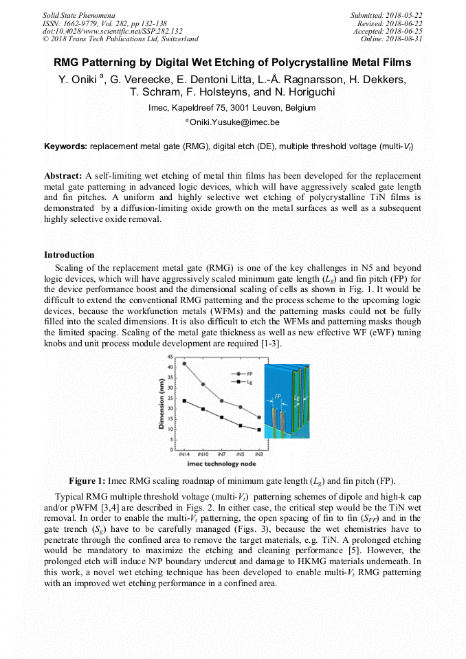
RMG Patterning by Digital Wet Etching of Polycrystalline Metal Films
p.132
p.132
Wet Etchants Penetration through Photoresist during Wet Patterning
p.141
p.141
Is Highly Selective Si3N4/SiO2 Etching Feasible without Phosphoric Acid?
p.147
p.147
Self-Aligned Contacting Processes for the 80 nm p-MTJ Device Fabrication by Wet Approach
p.152
p.152
Drying Stability and Critical Height of Repeating Line/Space Structures
p.161
p.161
RMG Patterning by Digital Wet Etching of Polycrystalline Metal Films

Abstract:
A self-limiting wet etching of metal thin films has been developed for the replacement metal gate patterning in advanced logic devices, which will have aggressively scaled gate length and fin pitches. A uniform and highly selective wet etching of polycrystalline TiN films is demonstrated by a diffusion-limiting oxide growth on the metal surfaces as well as a subsequent highly selective oxide removal.
You might also be interested in these eBooks
Info:
Periodical:
Solid State Phenomena (Volume 282)
Pages:
132-138
DOI:
Citation:
Online since:
August 2018
Price:
Сopyright:
© 2018 Trans Tech Publications Ltd. All Rights Reserved
Share:
Citation: