p.278
p.284
p.288
p.295
p.300
p.309
p.314
p.321
p.329
Yield Enhancement due to Addition of Bevel Cleans at Middle of Line(MOL) Zone
Abstract:
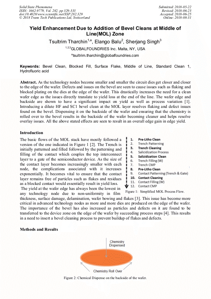
As the technology nodes become smaller and smaller the circuit dies get closer and closer to the edge of the wafer. Defects and issues on the bevel are seen to cause issues such as flaking and blocked plating on the dies at the edge of the wafer. This drastically increases the need for a clean wafer edge as the issues directly translate to yield loss at the end of the line. The wafer edge and backside are shown to have a significant impact on yield as well as process variation [1]. Introducing a dilute HF and SC1 bevel clean at the MOL layer resolves flaking and defect issues found on the bevel. Dispensing it on the backside of the wafer and ensuring that the chemistry is rolled over to the bevel results in the backside of the wafer becoming cleaner and helps resolve overlay issues. All the above stated effects are seen to result in an overall edge gain in edge yield.
Info:
Periodical:
Pages:
329-333
DOI:
Citation:
Online since:
August 2018
Authors:
Price:
Сopyright:
© 2018 Trans Tech Publications Ltd. All Rights Reserved
Share:
Citation:


