Bevel Mesa Combined with Implanted Junction Termination Structure for 10 kV SiC PiN Diodes

Article Preview

Abstract:

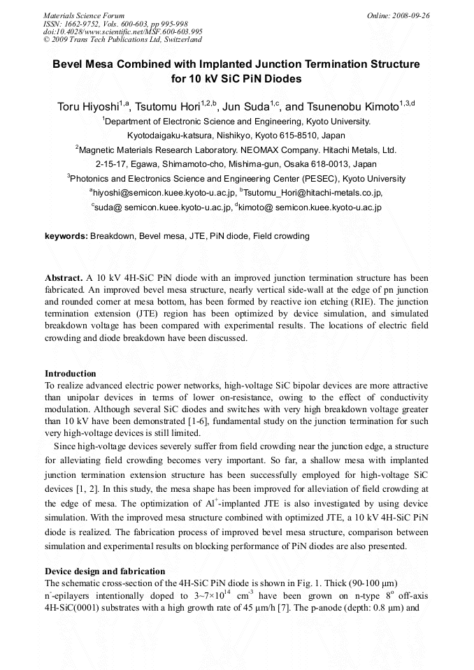
A 10 kV 4H-SiC PiN diode with an improved junction termination structure has been fabricated. An improved bevel mesa structure, nearly vertical side-wall at the edge of pn junction and rounded corner at mesa bottom, has been formed by reactive ion etching (RIE). The junction termination extension (JTE) region has been optimized by device simulation, and simulated breakdown voltage has been compared with experimental results. The locations of electric field crowding and diode breakdown have been discussed.

You might also be interested in these eBooks

Info:

Periodical:

Materials Science Forum (Volumes 600-603)

Pages:

995-998

Citation:

Online since:

September 2008

Export:

Price:

Permissions CCC:

Permissions PLS:

Сopyright:

© 2009 Trans Tech Publications Ltd. All Rights Reserved

Share:

Citation:

[1] Y. Sugawara, D. Takayama, K. Asano, R. Singh, J. W. Palmour, and T. Hayashi: Proc. of ISPSD (2001), p.27.

Google Scholar

[2] R. Singh, K. G. Irvine, J. T. Richmond, and J. W. Palmour: Mater. Sci. Forum Vol. 389-393 (2002), p.1265.

Google Scholar

[3] J. H. Zhao, P. Alexandrov, and X. Li: IEEE Electron Device Lett. Vol. 24 (2003), p.402.

Google Scholar

[4] J. H. Zhao, P. Alexandrov, and J. Zhang, and X. Li: IEEE Electron Device Lett. Vol. 25 (2004), p.474.

Google Scholar

[5] Q. Zhang, H-R. Chang, M. Gomez, C. Bui, E. Hanna, J. A. Higgins, T. Issacs-Smith, and J. R. Williams: Proc. of ISPSD (2005), p.303.

Google Scholar

[6] S. H. Ryu, S. Krishnaswami, B. Hull, J. Richmond, A. Agarwal, and A. Hefner: Proc. of ISPSD (2006), p.265.

Google Scholar

[7] T. Hori, K. Danno, and T. Kimoto: J. Crystal Growth Vol . 306 (2007), p.297.

Google Scholar

[8] Y. Negoro, K. Katsumoto, T. Kimoto, and H. Matsunami: J. Appl. Phys. Vol. 96 (2004), p.224.

Google Scholar

[9] Y. Negoro, T. Kimoto, and H. Matsunami: J. Appl. Phys. Vol. 98 (2005), p.043709.

Google Scholar