p.449
p.453
p.457
p.461
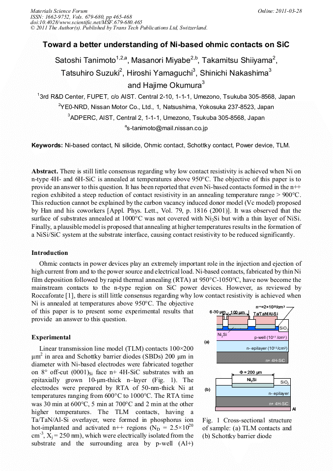
p.465
p.469
p.473
p.477
p.481
Toward a Better Understanding of Ni-Based Ohmic Contacts on SiC

Abstract:
There is still little consensus regarding why low contact resistivity is achieved when Ni on n-type 4H- and 6H-SiC is annealed at temperatures of more than above 950°C. The objective of this paper is to provide an answer concerning to this question. It is has been reported that even Ni-based contacts formed in the n++ region exhibited a steep reduction of contact resistivity in an annealing temperature range > 900°C. This effect reduction cannot be explained by the carbon vacancy induced donor model (Vc model) proposed by Han and his coworkers [Appl. Phys. Lett., Vol. 79, p. 1816 (2001)]. And, it is clarified that It was observed that the surface of substrates annealed at 1000°C was not covered with not Ni2Si but with a thin layer of NiSi. Finally, a plausible model is proposed that as the result of annealing at higher temperatures, results in the formation of the a NiSi/SiC system is builtat the substrate interface, resulting in significant reduction in low causing contact resistivity to be reduced significantly.
Info:
Periodical:
Pages:
465-468
Citation:
Online since:
March 2011
Keywords:
Permissions:
Share:
Citation: