p.461
p.465
p.469
p.473
p.477
p.481
p.485
p.489
p.493
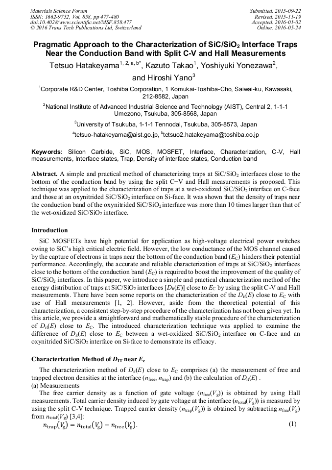
Pragmatic Approach to the Characterization of SiC/SiO2 Interface Traps near the Conduction Band with Split C-V and Hall Measurements
Abstract:
A simple and practical method of characterizing traps at SiC/SiO2 interfaces close to the bottom of the conduction band by using the split C−V and Hall measurements is proposed. This technique was applied to the characterization of traps at a wet-oxidized SiC/SiO2 interface on C-face and those at an oxynitrided SiC/SiO2 interface on Si-face. It was shown that the density of traps near the conduction band of the oxynitrided SiC/SiO2 interface was more than 10 times larger than that of the wet-oxidized SiC/SiO2 interface.
Info:
Periodical:
Pages:
477-480
DOI:
Citation:
Online since:
May 2016
Authors:
Price:
Сopyright:
© 2016 Trans Tech Publications Ltd. All Rights Reserved
Share:
Citation:


