p.549
p.553
p.557
p.561
p.565
p.569
p.573
p.577
p.585
Low Thermal Budget Ohmic Contact Formation by Laser Anneal

Abstract:
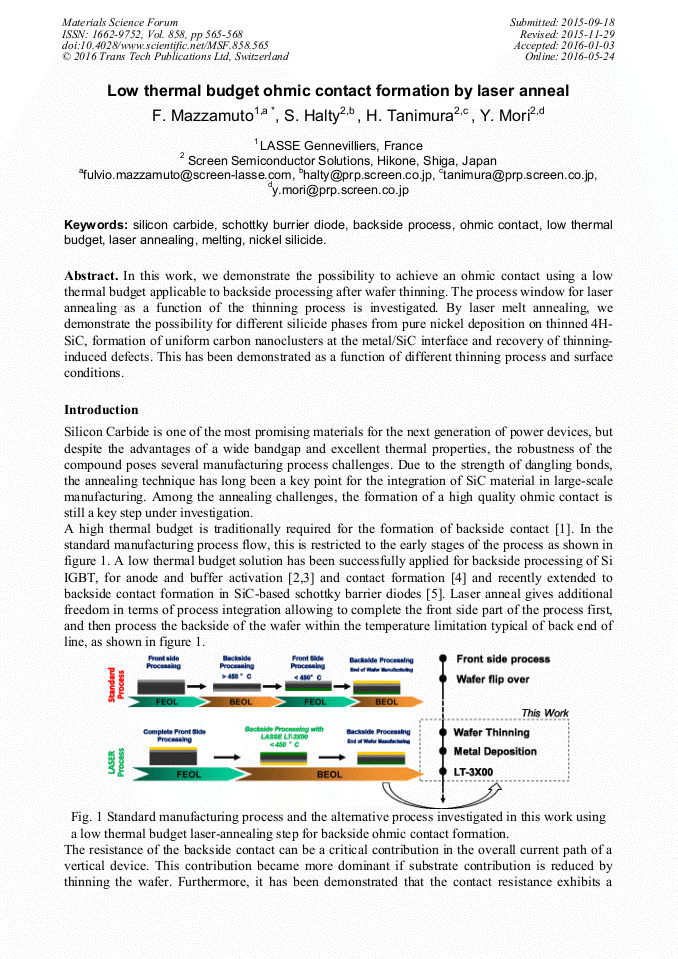
In this work, we demonstrate the possibility to achieve an ohmic contact using a low thermal budget applicable to backside processing after wafer thinning. The process window for laser annealing as a function of the thinning process is investigated. By laser melt annealing, we demonstrate the possibility for different silicide phases from pure nickel deposition on thinned 4H-SiC, formation of uniform carbon nanoclusters at the metal/SiC interface and recovery of thinning-induced defects. This has been demonstrated as a function of different thinning process and surface conditions.

Info:
Periodical:
Pages:
565-568
DOI:
Citation:
Online since:
May 2016
Authors:
Price:
Сopyright:
© 2016 Trans Tech Publications Ltd. All Rights Reserved
Share:
Citation: