Etching Rate Behavior of 4H-Silicon Carbide Epitaxial Film Using Chlorine Trifluoride Gas
p.715
p.715
Development of “Si-Vapor Etching” and “Si Vapor Ambient Anneal” in TaC/Ta Composite Materials
p.719
p.719
Novel 3C-SiC Microstructure for MEMS Applications
p.723
p.723
Study of 4H-SiC Junction Barrier Schottky(JBS) Diode Using Various Junction Structures
p.733
p.733
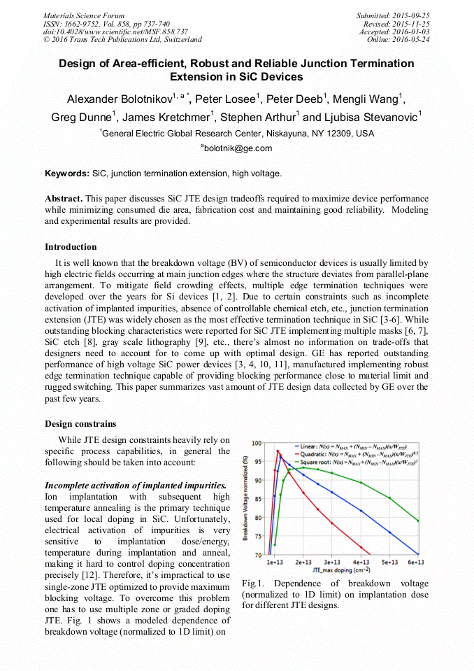
Design of Area-Efficient, Robust and Reliable Junction Termination Extension in SiC Devices
p.737
p.737
Modeling of Inhomogeneous 4H-SiC Schottky and JBS Diodes in a Wide Temperature Range
p.741
p.741
Optimum Design of 4H-SiC Junction Barrier Schottky Diode with Consideration of the Anisotropic Impact Ionization
p.745
p.745
Anomalous Scatter of Forward Current-Voltage Characteristics of He+-Irradiated Ni/4H-SiC Schottky Diodes
p.749
p.749
Epitaxial Layer Thickness Dependence on Heavy Ion Induced Charge Collection in 4H-SiC Schottky Barrier Diodes
p.753
p.753
Design of Area-Efficient, Robust and Reliable Junction Termination Extension in SiC Devices

Abstract:
This paper discusses SiC JTE design tradeoffs required to maximize device performance while minimizing consumed die area, fabrication cost and maintaining good reliability. Modeling and experimental results are provided.
You might also be interested in these eBooks

Info:
Periodical:
Materials Science Forum (Volume 858)
Pages:
737-740
DOI:
Citation:
Online since:
May 2016
Price:
Сopyright:
© 2016 Trans Tech Publications Ltd. All Rights Reserved
Share:
Citation: