Electrophoretic Studies on Silicon Nitride: Traces of Silicates in UPW Shift Zeta Potential Similar to SC-1
p.163
p.163
Damage-Free Cleaning of Sub-50 nm Devices Using Directed Megasonics Technology in a Single Wafer Processor
p.167
p.167
A Comparison of Particle Filtration in a Recirculated Wet Bench Wet Cleaning Tool: Performance of PTFE Filters and of Surface Optimized Filters
p.171
p.171
Influences of Oxide Loss on Contamination Removal
p.177
p.177
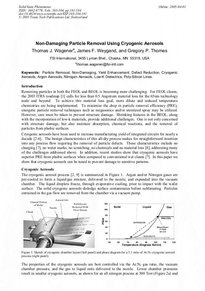
Non-Damaging Particle Removal Using Cryogenic Aerosols
p.181
p.181
Laser Cleaning of Particles from Silicon Wafers: Capabilities and Mechanisms
p.185
p.185
Contaminants Removal from Epi Substrates Using Vapor-Laser Process
p.189
p.189
Chemical Additive Formulations for Particle Removal in SCCO2-Based Cleaning
p.193
p.193
Non-Damaging CO2 Aerosol Cleaning in FEOL IC Manufacturing
p.199
p.199
Non-Damaging Particle Removal Using Cryogenic Aerosols

Abstract:
You might also be interested in these eBooks
Info:
Periodical:
Solid State Phenomena (Volumes 103-104)
Pages:
181-184
Citation:
Online since:
April 2005
Authors:
Price:
Сopyright:
© 2005 Trans Tech Publications Ltd. All Rights Reserved
Share:
Citation: