Deep-Ultraviolet Laser-Based Defect Inspection of Single-Crystal 4H-SiC and SmartSiCTM Engineered Substrates for High Volume Manufacturing

Article Preview

Abstract:

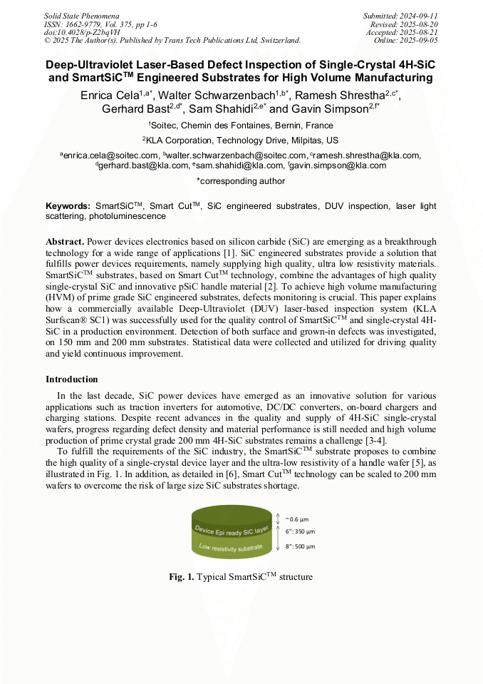
Power devices electronics based on silicon carbide (SiC) are emerging as a breakthrough technology for a wide range of applications [1]. SiC engineered substrates provide a solution that fulfills power devices requirements, namely supplying high quality, ultra low resistivity materials. SmartSiCTM substrates, based on Smart CutTM technology, combine the advantages of high quality single-crystal SiC and innovative pSiC handle material [2]. To achieve high volume manufacturing (HVM) of prime grade SiC engineered substrates, defects monitoring is crucial. This paper explains how a commercially available Deep-Ultraviolet (DUV) laser-based inspection system (KLA Surfscan® SC1) was successfully used for the quality control of SmartSiCTM and single-crystal 4H-SiC in a production environment. Detection of both surface and grown-in defects was investigated, on 150 mm and 200 mm substrates. Statistical data were collected and utilized for driving quality and yield continuous improvement.

You have full access to the following eBook

Info:

* - Corresponding Author

[1] T. Kimoto, Jpn. J. Appl. Phys. 54 040103 (2015).

Google Scholar

[2] C. Maleville, "SmartSiC™: a greener, faster and better technology for SiC" ICSCRM Conference, 2023.

Google Scholar

[3] M. Musolino et al., Microelectronic Engineering 274, 111976 (2023).

Google Scholar

[4] I. Manning et al., Mat. Sc. Forum 1062 (2022), pp.54-58.

Google Scholar

[5] S. Rouchier et al. "150 mm SiC engineered substrates for high-voltage power devices" ICSCRM Conference, 2021.

Google Scholar

[6] W. Schwarzenbach et al., "SmartSiCTM: Boosting SiC performance for high-voltage power applications," ICSCRM 2022.

Google Scholar

[7] E. Cela et al., Defect and diffusion forum 425 (2023), pp.57-61.

Google Scholar

[8] R. Brun et al., in Proceedings of the 2012 SEMI Advanced Semiconductor Manufacturing Conference, p.67.

Google Scholar

[9] J. Fan and P. K. Chu, Silicon Carbide Nanostructures, (Springer International Publishing Switzerland, 2014) pp.35-37.

Google Scholar

[10] T.Kimoto and J. A. Cooper, Fundamentals of Silicon Carbide Technology, (John Wiley and Sons, Singapore, 2014) p.51.

Google Scholar

[11] E. Cela et al., "Crystal originated defect monitoring and reduction in production grade SmartSiC™ engineered substrates." ICSCRM Conference, 2023.

DOI: 10.4028/p-s85vke

Google Scholar

[12] T.Kimoto and J. A. Cooper, Fundamentals of Silicon Carbide Technology, (John Wiley and Sons, Singapore, 2014) pp.147-149.

Google Scholar