Metal/P-GaN Contacts on AlGaN/GaN Heterostructures for Normally-Off HEMTs

Article Preview

Abstract:

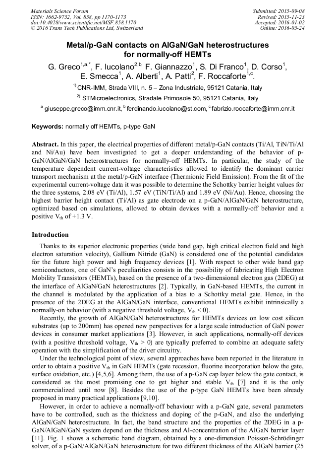
In this paper, the electrical properties of different metal/p-GaN contacts (Ti/Al, TiN/Ti/Al and Ni/Au) have been investigated to get a deeper understanding of the behavior of p-GaN/AlGaN/GaN heterostructures for normally-off HEMTs. In particular, the study of the temperature dependent current-voltage characteristics allowed to identify the dominant carrier transport mechanism at the metal/p-GaN interface (Thermionic Field Emission). From the fit of the experimental current-voltage data it was possible to determine the Schottky barrier height values for the three systems, 2.08 eV (Ti/Al), 1.57 eV (TiN/Ti/Al) and 1.89 eV (Ni/Au). Hence, choosing the highest barrier height contact (Ti/Al) as gate electrode on a p-GaN/AlGaN/GaN heterostructure, optimized based on simulations, allowed to obtain devices with a normally-off behavior and a positive Vth of +1.3 V.
You might also be interested in these eBooks

Info:

Periodical:

Pages:

1170-1173

Citation:

Online since:

May 2016

Export:

Price:

Permissions CCC:

Permissions PLS:

Сopyright:

© 2016 Trans Tech Publications Ltd. All Rights Reserved

Share:

Citation:

* - Corresponding Author

[1] F. Ren, J.C. Zolper, Wide Energy Bandgap Electronic Devices, World Scientific, Singapore, (2003).

Google Scholar

[2] M. Asif Khan, J.M. Van Hove, J.N. Kuznia, D.T. Olson, Appl. Phys. Lett. 58 (1991) 2408.

Google Scholar

[3] S. Tripathy, et al. , Appl. Phys. Lett. 101 (2012) 082110.

Google Scholar

[4] Y. Cai et al., IEEE Electron Device Lett. 53, (2006) 2207.

Google Scholar

[5] W. Saito et al., IEEE Electron Device Lett. 53, (2006) 356.

Google Scholar

[6] C.Y. Chang, et al. Appl. Phys. Lett. 94, (2009) 263505.

Google Scholar

[7] Y. Uemoto, et al., IEEE Trans. Electron Devices 54 (2007) 3393.

Google Scholar

[8] http: /epc-co. com; http: /www. gansystems. com.

Google Scholar

[9] T. Morita, et al., Proc. IEEE App. Power Electr. Conf. and Expo., Mar. 2011, pp.481-483.

Google Scholar

[10] T. Morita et al., in Proc. IEEE Int. Electr. Dev. Meeting, Dec. 2012, p.7. 2. 1–7. 2. 4.

Google Scholar

[11] O. Hilt et al., Proc. Int. Symp. Power Semicond. Devices ICs, Jun. 2010, pp.347-350.

Google Scholar

[12] I. Hwang et al., IEEE Electron Device Lett. 34, (2013) 202.

Google Scholar

[13] F. Lee et al., IEEE Electron Device Lett. 36, (2015) 232.

Google Scholar

[14] M. Marso, et al., Electron. Lett. 31, (1995) 589.

Google Scholar

[15] F. Iucolano et al., Appl. Phys. Lett. 103, (2013) 201604.

Google Scholar

[16] Y.J. Lin, C.T. Lee, S.S. Chang and H.C. Chang, J. Phys. D: Appl. Phys. 41, (2008) 095107.

Google Scholar

[17] G. Greco et al., J. Appl. Phys. 110, (2011) 123703.

Google Scholar

[18] J. S. Kwak, O. H. Nam, and Y. Park, Appl. Phys. Lett. 80, (2002) 3554.

Google Scholar

[19] K. Shiojima, T. Sugahara, and S. Sakai, Appl. Phys. Lett. 77, (2000) 4353.

Google Scholar

[20] J. S. Kwak, O. H Nam, and Y. Park, J. Appl. Phys., 95, (2004) 5917.

Google Scholar