p.498
p.504
p.509
p.514
p.519
p.523
p.528
p.533
p.539
DC Modeling of 4H-SiC nJFET Gate Length Reduction at 500°C

Abstract:
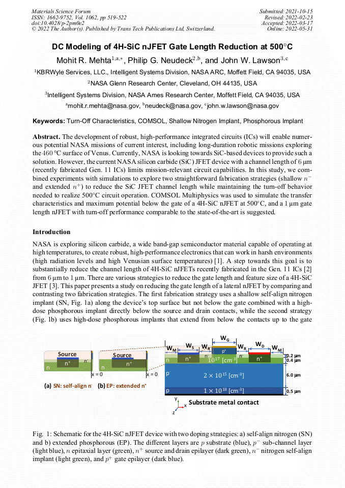
The development of robust, high-performance integrated circuits (ICs) will enable numerous potential NASA missions of current interest, including long-duration robotic missions exploring the 460°C surface of Venus. Currently, NASA is looking towards SiC-based devices to provide such a solution. However, the current NASA silicon carbide (SiC) JFET device with a channel length of 6 μm (recently fabricated Gen. 11 ICs) limits mission-relevant circuit capabilities. In this study, we combined experiments with simulations to explore two straightforward fabrication strategies (shallow n−and extended n+) to reduce the SiC JFET channel length while maintaining the turn-off behavior needed to realize 500°C circuit operation. COMSOL Multiphysics was used to simulate the transfer characteristics and maximum potential below the gate of a 4H-SiC nJFET at 500°C, and a 1 μm gate length nJFET with turn-off performance comparable to the state-of-the-art is suggested.

Info:
Periodical:
Pages:
519-522
DOI:
Citation:
Online since:
May 2022
Authors:
Permissions:
Share:
Citation: