High Power-Density 4H-SiC RF MOSFETs
p.1277
p.1277
4.3 mΩcm2, 1100 V 4H-SiC Implantation and Epitaxial MOSFET
p.1281
p.1281
Fabrication and Performance of 1.2 kV, 12.9 mΩcm2 4H-SiC Epilayer Channel MOSFET
p.1285
p.1285
Switching Characteristics of SiC-MOSFET and SBD Power Modules
p.1289
p.1289
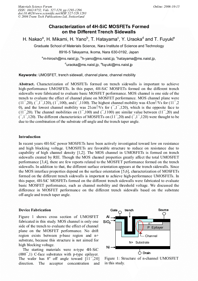
Characterization of 4H-SiC MOSFETs Formed on the Different Trench Sidewalls
p.1293
p.1293
The Characteristics of MOSFETs Fabricated on the Trench Sidewalls of Various Faces Using 4H-SiC (11-20) Substrates
p.1297
p.1297
Fabrication of 4H-SiC p-Channel MOSFET with High Channel Mobility
p.1301
p.1301
Reduction of On-Resistance in 4H-SiC Multi-RESURF MOSFETs
p.1305
p.1305
Fabrication of 4H-SiC DIMOSFETs by High-Temperature (>1400°C) Rapid Thermal Oxidation and Nitridation Using Cold-Wall Oxidation Furnace
p.1309
p.1309
Characterization of 4H-SiC MOSFETs Formed on the Different Trench Sidewalls

Abstract:
You might also be interested in these eBooks
Info:
Periodical:
Materials Science Forum (Volumes 527-529)
Pages:
1293-1296
Citation:
Online since:
October 2006
Keywords:
Price:
Сopyright:
© 2006 Trans Tech Publications Ltd. All Rights Reserved
Share:
Citation: