Reduction of On-Resistance in 4H-SiC Multi-RESURF MOSFETs

Article Preview

Abstract:

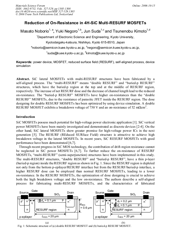
SiC lateral MOSFETs with multi-RESURF structures have been fabricated by a self-aligned process. The “multi-RESURF” means “double RESURF” and “buried-p RESURF” structures, which have the buried-p region at the top and at the middle of RESURF region, respectively. The increase of net RESURF dose and the decrease of channel length lead to the reduced on-resistance. The “buried-p RESURF” MOSFETs have higher on-resistances than the “double RESURF” MOSFETs, due to the resistance of parasitic JFET inside the RESURF region. The dose designing for double RESURF MOSFETs has been optimized by using device simulation. A double RESURF MOSFET exhibits a breakdown voltage of 750 V and an on-resistance of 52 m/cm2.

You might also be interested in these eBooks

Info:

Periodical:

Materials Science Forum (Volumes 527-529)

Pages:

1305-1308

Citation:

Online since:

October 2006

Export:

Price:

Permissions CCC:

Permissions PLS:

Сopyright:

© 2006 Trans Tech Publications Ltd. All Rights Reserved

Share:

Citation:

[1] J.A. Cooper, M.R. Melloch, R. Singh, A. Agarwal, and J.W. Palmour: IEEE Trans. Electron Devices, Vol. 49 (2002), p.658.

DOI: 10.1109/16.992876

Google Scholar

[2] S.H. Ryu, S. Krishnaswami, M. O'Loughlin, J. Richmond, A. Agarwal, J. Palmour, and A. R. Hefner: IEEE Electron Device Lett., Vol. 25 (2004), p.556.

Google Scholar

[3] D. Peters, R. Schırner, P. Friedrichs, and D. Stephani: Mater. Sci. Forum, Vols. 433-436 (2003), p.769.

Google Scholar

[4] M. Matin, A. Saha, and J.A. Cooper: IEEE Trans. Electron Devices, Vol. 51 (2004), p.1721.

Google Scholar

[5] K. Chatty, S. Banerjee, T.P. Chow, and R.J. Gutmann: IEEE Electron Device Lett., Vol. 21 (2000), p.356.

Google Scholar

[6] S. Banerjee, T.P. Chow, and R.J. Gutmann: IEEE Electron Device Lett., Vol. 23 (2002), p.624.

Google Scholar

[7] T. Kimoto, H. Kawano, and J. Suda: IEEE Electron Device Lett., Vol. 26 (2005), p.649.

Google Scholar

[8] Y. Negoro, K. Katsumoto, T. Kimoto, and H. Matsunami: J. Appl. Phys., Vol. 96 (2004), p.224.

Google Scholar

[9] L.A. Lipkin, M.K. Das, and J.W. Palmour: Mater. Sci. Forum, Vols. 389-393 (2002), p.985.

Google Scholar