Single-Wafer Wet Chemical Oxide Formation for Pre-ALD High-k Deposition on 300 mm Wafer
p.53
p.53
Effect of SC-1 Treatment in Thermal Wall Oxide on Nanoscale STI Gap-Filling by O3/TEOS CVD
p.57
p.57
Etch Rate Profile Characterization of High-κ Materials
p.63
p.63
Critical Thickness Threshold in HfO2 Layers
p.67
p.67
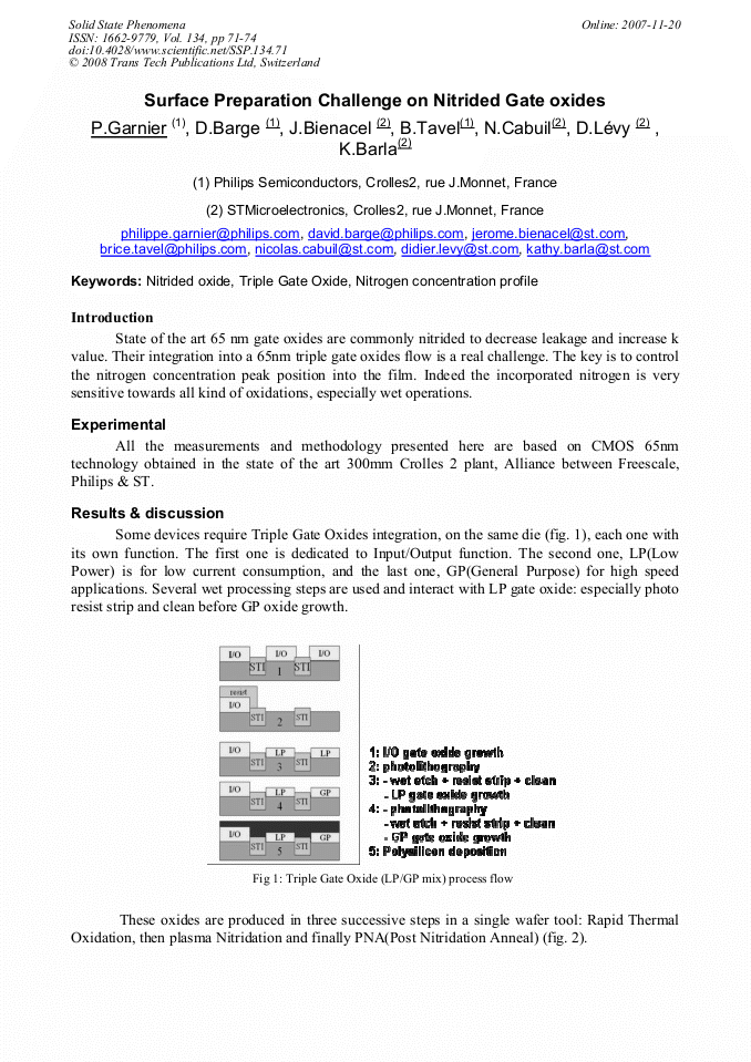
Surface Preparation Challenge on Nitrided Gate Oxides
p.71
p.71
Development of a New TaN Etchant for Metal Gate
p.75
p.75
Peracetic Acid as Active Species in Mixtures for Selective Etching of SiGe/Si Layer Systems – Aspects of Chemistry and Analytics
p.79
p.79
A Wet Etching Technique to Reveal Threading Dislocations in Thin Germanium Layers
p.83
p.83
Galvanic Corrosion of Stacked Metal Gate Electrodes during Cleaning in HF Solutions
p.87
p.87
Surface Preparation Challenge on Nitrided Gate Oxides

Abstract:
You might also be interested in these eBooks
Info:
Periodical:
Solid State Phenomena (Volume 134)
Pages:
71-74
DOI:
Citation:
Online since:
November 2007
Price:
Сopyright:
© 2008 Trans Tech Publications Ltd. All Rights Reserved
Share:
Citation: