Comparative Study of 1.2kV 4H-SiC Bi-Directional MOSFET (BiD-MOS) Design Approaches: 2-Chip vs Monolithic Integration
p.37
p.37
Characteristics of High Current 4H-SiC Schottky Barrier Diodes
p.45
p.45
Design Optimization of 600V 4H-SiC Lateral Bi-Directional MOSFET (L-BiD-MOSFET) with 3D TCAD Simulation
p.51
p.51
Design of the Robust Edge Termination Applied to 4.5 kV SiC SBD Embedded MOSFET against Humidity
p.57
p.57
JTE-Based Termination Design and Technology Considerations for 1500 V 4H-SiC Superjunction MOSFETs
p.63
p.63
2x Current Boosting Scheme in 3300 v 4H-SiC VDMOSFET
p.69
p.69
Study of Single-Event-Burnout for Refilled-PMOS SiC Trench MOSFET
p.75
p.75
Benchmark Study of State-of-the-Art Commercial 1200V SiC MOSFETs for Automotive Applications
p.85
p.85
Study of SiC Thyristors with Integrated Temperature Sensors
p.93
p.93
2x Current Boosting Scheme in 3300 v 4H-SiC VDMOSFET

Abstract:
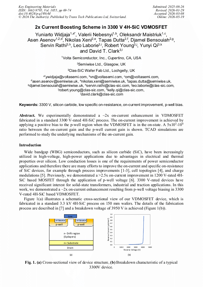
We experimentally demonstrated a ~2x on-current enhancement in VDMOSFET fabricated in a standard 3300 V-rated 4H-SiC process. The on-current improvement is achieved by applying a positive bias to the p-well region when the VDMOSFET is in the on-state. A 5x10³-104 ratio between the on-current gain and the p-well current gain is shown. TCAD simulations are performed to study the underlying mechanisms of the on-current gain.
You have full access to the following eBook
Info:
Periodical:
Key Engineering Materials (Volume 1055)
Pages:
69-74
DOI:
https://doi.org/10.4028/p-q19NrM
DOI link
Citation:
Online since:
May 2026
Permissions:
Share:
Citation: