p.1
p.9
p.17
p.27
p.33
p.41
p.47
p.53
Isolation Structure for Monolithic Integration of Planar CMOS and 1.7 kV Vertical Power MOSFET on 4H-SiC by High Energy Ion Implantation

Abstract:
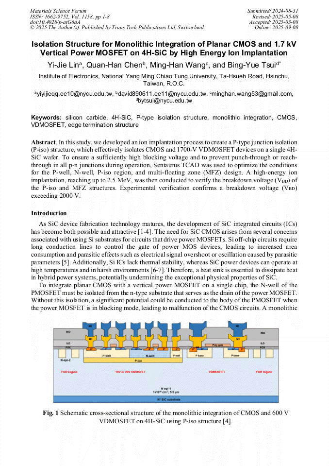
In this study, we developed an ion implantation process to create a P-type junction isolation (P-iso) structure, which effectively isolates CMOS and 1700-V VDMOSFET devices on a single 4H-SiC wafer. To ensure a sufficiently high blocking voltage and to prevent punch-through or reach-through in all p-n junctions during operation, Sentaurus TCAD was used to optimize the conditions for the P-well, N-well, P-iso region, and multi-floating zone (MFZ) design. A high-energy ion implantation, reaching up to 2.5 MeV, was then conducted to verify the breakdown voltage (VBD) of the P-iso and MFZ structures. Experimental verification confirms a breakdown voltage (VBD) exceeding 2000 V.

Info:
Periodical:
Pages:
1-8
DOI:
Citation:
Online since:
September 2025
Authors:
Permissions:
Share:
Citation: