Rapid Thermal Anneal with Conductive Heating for SiC Contact Formation
p.33
p.33
The Investigation of Effective Thermal Oxidation to SiC MOSFET Gate Oxide Quality Improvement
p.41
p.41
A Simplified Method for Extracting Contact Resistivity Using the Circular Transmission Line Model
p.47
p.47
BCl3 Plasma Treatment for Enhanced Ohmic Contact Performance to p-Type 4H-SiC
p.53
p.53
Advantages of Backside Metal Contact Resistance on 4H-SiC Bonded Substrates for Power Devices
p.59
p.59
Investigation of Interface and Reliability of 3C- and 4H-SiC MOS Structures through Gate Dielectric Stacking and Post-Deposition Annealing
p.67
p.67
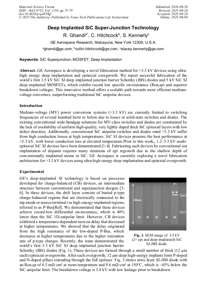
Deep Implanted SiC Super-Junction Technology
p.75
p.75
Improved Angle Tolerance in 4H-SiC Trench Filling Epitaxy Using Chlorinated Chemistry
p.81
p.81
Study of SiC Trench Etching Characteristics for Different Crystal Planes
p.87
p.87
Deep Implanted SiC Super-Junction Technology

Abstract:
GE Aerospace is developing a novel fabrication method for >3.3 kV devices using ultra-high energy deep implantation and epitaxial overgrowth. We report succesful fabrication of the world’s first 3.5 kV SiC SJ deep implanted junction barrier Schottky (JBS) diodes and 5 kV SiC SJ deep implanted MOSFETs, which exhibit record low specific on-resistance (Ron,sp) and superior breakdown voltages. This innovative method offers a scalable path towards more efficient medium-voltage converters, outperforming traditional SiC unipolar devices.
You have full access to the following eBook
You might also be interested in these eBooks

Info:
Periodical:
Materials Science Forum (Volume 1158)
Pages:
75-79
DOI:
https://doi.org/10.4028/p-qAFI4Q
DOI link
Citation:
Online since:
September 2025
Authors:
Keywords:
Permissions:
Share:
Citation: